- 您现在的位置:买卖IC网 > Sheet目录983 > HI5714EVAL (Intersil)EVALUATION PLATFORM HI5714
�� �
�
�Application� Note� 9517�
�Control� Amplifier� to� provide� adequate� drive� for� the�
�segmented� current� cells� and� the� R2/R� resistor� ladder.�
�Reference� Out� (REF� OUT)� should� be� connected� to� the�
�Control� Amplifier� Input� (CTRL� AMP� IN).� The� Control�
�Amplifier� Output� (CTRL� AMP� OUT)� should� be� used� to� drive�
�the� Reference� Input� (REF� IN)� and� a� 0.1� μ� F� capacitor� to�
�analog� V-(-AV� EE� ).� This� improves� settling� time� by� decoupling�
�switching� noise� from� the� analog� output� of� the� HI5721.�
�The� Full� Scale� Output� Current� is� controlled� by� the� CTRL�
�AMP� IN� pin� and� the� set� resistor� (R� SET� ).� The� ratio� is:�
�I� OUT� (Full� Scale)� =� (CTRL� AMP� IN/R� SET� )� x� 32�
�The� outputs� I� OUT� and� I� OUT� are� complementary� current�
�outputs.� Current� is� steered� to� either� I� OUT� or� I� OUT� in�
�proportion� to� the� digital� input� code.� The� sum� of� the� two�
�currents� is� always� equal� to� the� full� scale� current� minus� one�
�LSB.� The� current� output� can� be� converted� to� a� voltage� by�
�using� a� resistor� load.� Both� current� outputs� should� have� the�
�same� load� (50� ?� typically).� The� output� voltage� is:�
�V� OUT� =� I� OUT� x� R� OUT�
�The� compliance� range� of� the� outputs� is� from� -1.5V� to� +3.0V.�
�HI5714� Characterization�
�Various� tests� can� be� used� to� characterize� the� performance�
�of� the� HI5714.� The� integral� nonlinearity� (INL)� and� differential�
�nonlinearity� (DNL)� specs� are� considered� a� measure� of� the�
�low� frequency� characteristics� of� the� ADC.� These� parameters�
�are� evaluated� at� the� factory� using� a� histogram� approach� with�
�a� low� frequency� ramp� input.�
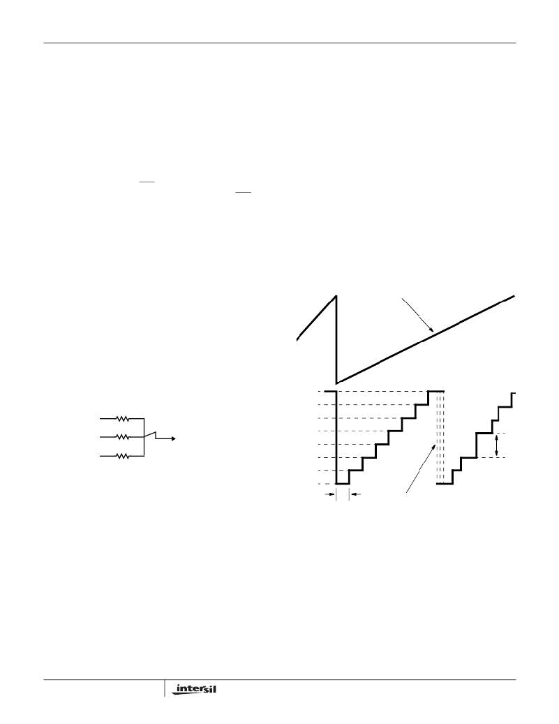
�A� three� bit� reconstruction� DAC,� as� shown� in� Figure� 7,� can� be�
�constructed� to� do� a� rough� evaluation� of� HI5714� for� DNL,�
�missing� codes,� and� transition� noise.�
�1K�
�DOUT2�
�For� example,� if� k� =� 10,� n� =� 8,� m� =� 16,� F� S� =� 20� MSPS,� and�
�FSR� =� 1V� then� the� input� ramp� would� have� a� V� P-P� of� 62.5mV�
�and� a� period� (T)� of� 8� μ� s.� To� view� the� reconstructed� output,�
�connect� the� X� axis� of� an� oscilloscope� to� the� ramp� input� and�
�the� Y� axis� would� be� connected� to� the� reconstruction� DAC�
�output.� Another� oscilloscope� could� be� used� to� probe� the� bits�
�to� verify� the� codes� that� are� being� tested.� The� analog� input�
�should� be� low� pass� filtered� to� remove� as� much� noise� as�
�possible.� Notice� that� the� input� ramp� is� only� covering� m� steps�
�out� a� possible� 2� n� possible� for� the� ADC.� Therefore,� the�
�generator� used� for� this� test� will� have� to� be� able� to� offset� the�
�input� through� the� range� of� the� converter� so� all� the� codes� for�
�the� ADC� can� be� inspected.�
�Figure� 8� shows� what� an� ideal� reconstructed� output� would�
�look� like� with� and� without� various� errors.� For� an� ideal� ADC�
�and� an� ideal� ramp� input,� the� digital� output� code� will� change�
�state� by� 1� LSB� every� kth� conversion� for� an� 1� LSB� change� on�
�the� input.� ADC� errors� will� make� the� codes� change� before� or�
�after� the� kth� conversion� and� will� translate� to� a� larger� or�
�smaller� step� width.� The� actual� step� width� size� would� be�
�compared� with� the� ideal� LSB� size� to� determine� errors.� Since�
�this� is� a� visual� comparison� it� will� tend� not� to� be� very� precise.�
�RAMP� INPUT�
�111�
�110�
�101�
�DOUT1�
�2K�
�4K�
�OSCILLOSCOPE�
�100�
�011�
�B�
�DOUT0�
�FIGURE� 7.� THREE� BIT� RECONSTRUCTION� DAC�
�010�
�001�
�The� input� frequency� is� set� so� that� the� input� will� changes� by�
�1� LSB� for� every� k� conversions� of� the� ADC.� The� p-to-p� voltage�
�of� the� staircase� is� then� determined� by� the� number� of� LSB�
�000�
�1� LSB�
�MAJOR� TRANSITION�
�NOISE�
�B� -� MISSING�
�CODE�
�V� P� –� P� =� ------------------------�
�m� � k�
�F� S�
�steps� within� one� period� of� the� input� ramp.� The� following�
�equations� can� be� used:�
�m� � FSR�
�2� n�
�T� =� --------------�
�Where:�
�F� S� =� sampling� frequency� of� the� ADC.�
�FSR� =� full� scale� range� of� the� ADC.�
�k� =� desired� test� resolution� (number� of� conversions� per� LSB).�
�m� =� desired� number� of� steps� (LSBs)� per� ramp� period.�
�n� =� number� of� bits� of� the� ADC.�
�4�
�FIGURE� 8.� THREE� BIT� DAC� WAVEFORMS�
�Further� dynamic� testing� is� used� to� evaluate� the� HI5714�
�performance� as� the� input� starts� to� approach� Nyquist� (F� S� /2).�
�Among� these� tests� are� Signal-to-Noise� Ratio� (SNR),� Signal-�
�to-Noise� And� Distortion� (SINAD),� and� Total� Harmonic�
�Distortion� (THD).�
�Coherent� testing� is� recommended� in� order� to� avoid� the�
�inaccuracies� due� to� windowing.� Coherent� sampling� is�
�governed� by� the� following� relationship:� F� T� /F� S� =� M/N.� Where�
�F� T� is� the� frequency� of� the� input� tone,� F� S� is� the� sampling�
�frequency,� N� is� the� number� of� samples,� and� M� is� the� number�
�of� cycles� over� which� the� samples� are� taken.� By� making� M� an�
�integer� and� prime� (1,� 3,� 5.� .� .)� the� samples� are� assured� of�
�发布紧急采购,3分钟左右您将得到回复。
相关PDF资料
HI5728EVAL1
EVALUATION PLATFORM TQFPHI5728
HI5731-EVS
EVALUATION PLATFORM SOIC HI5731
HI5741-EVS
EVALUATION PLATFORM HI5741
HI5760EVAL1
EVALUATION PLATFORM SOIC HI5760
HI5762EVAL2
EVALUATION MOD FOR HI5762 AMP
HI5767EVAL1
EVALUATION PLATFORM HI5767
HI5767EVAL2
EVALUATION PLATFORM HI5767
HI5805EVAL1
EVALUATION PLATFORM HI5805
相关代理商/技术参数
HI5721
制造商:INTERSIL 制造商全称:Intersil Corporation 功能描述:10-Bit, 125 MSPS, High Speed D/A Converter
HI5721 WAF
制造商:Harris Corporation 功能描述:
HI5721_03
制造商:INTERSIL 制造商全称:Intersil Corporation 功能描述:10-Bit, 125MSPS, High Speed D/A Converter
HI5721BIB
制造商:Rochester Electronics LLC 功能描述: 制造商:Harris Corporation 功能描述: 制造商:Intersil Corporation 功能描述:
HI5721BIBS2503
制造商:Rochester Electronics LLC 功能描述:- Bulk
HI5721BIB-T
制造商:Rochester Electronics LLC 功能描述:HI5721BIB IN TAPE & REEL - Bulk
HI5721BIB-TS5001
制造商:Rochester Electronics LLC 功能描述:- Bulk
HI5721BIP
制造商:Rochester Electronics LLC 功能描述:28 PDIP INDTEMP D/A 10 BIT 125 MHZ -5.2V - Bulk